
Efforts to seamlessly merge the digital world with our physical environment have consistently been hindered by the fundamental rigidity of conventional electronics, a problem that now has a promising and surprisingly simple solution. The development of a novel heat-shrinking method allows for the integration of high-performance electronic circuits onto almost any irregular, three-dimensional surface. This breakthrough addresses the long-standing limitations of traditional electronics, which are typically built on flat, stiff boards, making them ill-suited for the dynamic and curved shapes of the world around us. By creating a method to essentially “shrink-wrap” circuits onto objects, this research opens a new frontier for smart devices that can conform perfectly to their surroundings.
A Novel Approach to Flexible Electronics
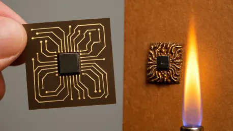
This research introduces an innovative technique that utilizes a standard thermoplastic film, which shrinks when heated, to serve as a substrate for electronic circuits. By printing circuits onto this film and then applying gentle heat, the material conforms snugly around complex objects, from the gentle curve of a piece of fruit to the intricate shape of an aircraft wing. This process effectively transforms a flat, two-dimensional circuit into a fully integrated three-dimensional electronic system, creating a seamless interface between technology and the physical object.
The ingenuity of this approach lies in its ability to overcome the primary obstacles that have plagued flexible electronics. Unlike methods that require complex manufacturing or specialized materials, this heat-shrinking technique is straightforward and relies on readily available components. It offers a practical and scalable solution for fabricating electronics that can adapt to non-uniform surfaces, moving beyond the flat plane that has defined electronics for decades and toward a future where technology is truly integrated into the fabric of our lives.
The Challenge of Conforming Electronics to the Real World
Traditional electronics are designed for a flat world. Their construction on rigid circuit boards makes them inherently incompatible with the soft, curved, and often moving surfaces that characterize real-world applications, such as the human body, robotics, or aerodynamic structures. This fundamental mismatch has created a significant barrier to developing wearable health monitors that are truly comfortable, sensors that can cover an entire aircraft wing, or smart packaging that fits perfectly around its contents. The inability to conform has limited the potential of smart technology in countless fields.
While various flexible alternatives have been developed to address this issue, they have often introduced their own set of problems. Many flexible circuits are fragile, prone to failure after repeated bending, or suffer from performance degradation. Furthermore, their manufacturing processes can be intricate and prohibitively expensive, preventing widespread adoption. The field has long been in need of a solution that balances flexibility with durability and performance, while also remaining simple and cost-effective enough for practical, large-scale use. This new research provides a direct and effective answer to these persistent challenges.
Research Methodology, Findings, and Implications
Methodology
The core of the methodology involved printing circuits onto a thermoplastic film using a specially formulated semi-liquid metal alloy. This alloy, a mixture of gallium, indium, and copper, possesses a unique set of properties crucial to the process’s success. It remains fluid enough to stretch and bend without breaking the electrical connection, yet it is also viscous enough to hold its precise, printed shape on the film without smudging or running. This material innovation solves the critical problem of wire snapping that would occur with conventional solid conductors like copper.
To ensure the circuits maintained their integrity and functionality after shrinking, the researchers employed advanced computer simulations. These simulations accurately predicted how the thermoplastic film would warp and deform when heated, allowing for the design of circuit patterns that would align perfectly on the final three-dimensional object. This predictive design step is essential for preventing distortion and ensuring the electronics function as intended.
Once the circuit was printed according to the computer-generated model, the final step was the heat application. By using a gentle stream of hot air or a bath of warm water, researchers could trigger the shrinking process. This caused the thermoplastic film to pull tight and conform flawlessly to the contours of the target object, effectively molding the liquid metal circuit into its final, three-dimensional form without causing any damage to the circuit or the object itself.
Findings
The durability of the resulting circuits was a key finding of the study. To test their resilience, the researchers subjected the shrink-fitted electronics to rigorous mechanical stress, including 5,000 cycles of repeated bending and twisting. Remarkably, the circuits demonstrated almost no change in their electrical conductivity throughout this extensive testing period. This level of robustness confirms that the semi-liquid metal can withstand the strains of real-world use far better than traditional solid wires, which would likely develop microcracks and fail under similar conditions.
The study conclusively demonstrated that this heat-shrinking method is not only durable but also a highly practical and cost-effective technique for fabricating shape-adaptive electronics. By leveraging common materials and a relatively simple process, the researchers have developed a scalable solution that stands in stark contrast to the complex and expensive manufacturing required for other flexible electronic technologies. This combination of high performance, durability, and affordability validates the method as a significant advancement in the field.
Implications
The technology’s potential was showcased through a series of successful real-world applications. In one test, researchers created smart bandages capable of monitoring their own status, which could have significant implications for wound care and remote patient monitoring. Another application involved shrinking sensors onto fresh fruit to track temperature and humidity, offering a powerful new tool for improving food safety and reducing waste in the agricultural supply chain.
Furthermore, the team integrated a de-icing heating system onto a model aircraft wing, demonstrating the technology’s potential in the aerospace industry, where preventing ice buildup is critical for safety. The sheer versatility of this method suggests that its implications are vast, opening up new possibilities in fields ranging from advanced medical devices and consumer electronics to agriculture and industrial monitoring. This technique provides a foundational platform for developing a new class of smart, integrated devices.
Reflection and Future Directions
Reflection
The study’s success hinged on overcoming two significant technical hurdles that have historically limited the development of conformable electronics. The first was the inherent risk of conductive pathways snapping or breaking when the underlying material is stretched or shrunk. This was elegantly solved by the use of the semi-liquid metal alloy, which could flow and deform along with the thermoplastic film without losing its electrical integrity, ensuring a continuous and reliable connection.
The second major challenge was the unpredictable and often chaotic way that a material can warp and wrinkle as it shrinks. Without precise control, any pre-printed circuit would become hopelessly distorted and non-functional. The researchers addressed this by using predictive computer simulations to model the shrinking process. This allowed them to pre-distort the circuit design on the flat film in such a way that it would resolve into the correct, precise pattern once conformed to the final three-dimensional shape.
Future Directions
Looking ahead, the research team plans to refine and expand upon this breakthrough method. A primary focus will be on enhancing the precision of the technique to allow for the application of circuits to an even wider range of highly complex and intricate shapes and surfaces. This could involve developing more sophisticated simulation models and improving the printing process to accommodate finer circuit details, enabling more advanced electronic functionalities.
Future exploration will also likely concentrate on expanding the types of electronic components that can be integrated using this method. While the current research focuses on conductive pathways and simple sensors, the goal is to incorporate a broader array of components, such as microcontrollers, transistors, and wireless communication modules. Achieving this would enable the creation of fully autonomous, complex electronic systems that can be shrink-fitted onto virtually any object, further blurring the line between the physical and digital worlds.
Revolutionizing How Electronics Integrate with Our World
This research delivered a simple, durable, and cost-effective method for creating electronics that fit the complex shapes of the world we live in. By establishing a practical way to “shrink-wrap” circuits onto almost any surface, this breakthrough has laid the groundwork for a new generation of smart devices. The implications of this work suggest a future where technology is no longer confined to rigid boxes but is seamlessly and invisibly integrated into the objects we use every day, from smarter medical implants and more efficient aircraft to everyday consumer goods.