
The relentless expansion of artificial intelligence applications has finally pushed the physical limits of traditional silicon, forcing a radical departure from the architectures that have defined computing for decades. As developers strive for instantaneous processing in autonomous systems and mobile devices, the “von Neumann bottleneck”—the lag created by moving data between separate memory and processing units—has become an unsustainable drain on both time and power. To resolve this, the industry is pivoting toward in-memory computing, a paradigm where data is processed exactly where it is stored. At the heart of this transition lies the ferroelectric transistor, a component capable of non-volatile storage and rapid switching, yet its success depends entirely on how engineers manipulate the crystal structure of Hafnium Oxide ($HfO_2$).
Material Modulation in Next-Generation AI Semiconductors
The evolution of AI hardware has reached a critical juncture where software complexity no longer just demands more transistors, but fundamentally different ones. Traditional chips are struggling to keep pace with the massive parallel processing required for modern neural networks, leading to a surge in research into ferroelectric materials. These materials are prized for their ability to maintain an electric polarization that can be reversed by an external electric field, allowing them to function as high-speed, low-energy memory. However, the efficacy of these devices depends on achieving a specific “orthorhombic” crystal phase within the Hafnium Oxide, a task that becomes increasingly difficult as the industry pushes for smaller, thinner semiconductor films.
Professor Taesung Kim and his research team at Sungkyunkwan University have recently spotlighted this challenge, focusing on how to stabilize Hafnium Oxide at the atomic scale. While the material is already a staple in semiconductor fabrication due to its high dielectric constant, its ferroelectric properties are notoriously fickle. For years, the industry has relied on chemical doping to force the material into the correct alignment. However, the Sungkyunkwan team has introduced a competing strategic purpose: thermal constraining. This method moves away from chemical additives and instead uses physical mechanics to lock the crystal structure in place, offering a potentially more reliable foundation for the future of non-volatile memory in AI.
Technical Mechanisms and Performance Metrics
Lattice Engineering and Structural Stability
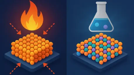
The fundamental difference between these two paths lies in whether the material is altered from the inside out or the outside in. Chemical doping involves the traditional method of introducing foreign elements—such as aluminum or lanthanum—into the Hafnium Oxide lattice to disrupt the natural tendency of the atoms to settle into a non-ferroelectric monoclinic phase. In contrast, the thermal constraining approach functions like a physical mold, a concept the researchers liken to the “bungeoppang” or fish-shaped pastry mold used in Korean street food. By using tungsten electrodes to encase the $HfO_2$ during the annealing process, the difference in thermal expansion rates between the metal and the oxide creates a powerful compressive force.
This “thermal force” physically prevents the atoms from shifting out of the desired orthorhombic phase. While chemical doping often fails in ultra-thin films because the dopants can migrate or fail to provide enough structural tension at smaller scales, thermal expansion engineering maintains its grip regardless of thickness. By leveraging the specific physical properties of tungsten, the thermal constraining method ensures that the atomic alignment remains locked. This prevents the reversion to less useful crystal phases that typically plagues chemically modified films as they shrink toward the atomic limit.
Scalability and Manufacturing Consistency
When moving from a laboratory setting to a high-volume fabrication plant, production complexity becomes a deciding factor. Chemical doping requires extreme precision; even a slight variance in the concentration of dopants can lead to inconsistent switching behavior across a wafer. This sensitivity adds layers of complexity to the manufacturing chain, requiring sophisticated control systems to ensure every batch meets rigorous standards. The physical stress-modulated method pioneered by the Sungkyunkwan University team simplifies this process significantly. By relying on the inherent physical properties of the electrode materials, manufacturers can achieve the necessary lattice distortion through standard heating and cooling cycles.
Integration with existing infrastructure is another area where thermal constraining shows significant promise. Because it utilizes tungsten—a material already widely used in semiconductor manufacturing—it does not require the introduction of exotic or potentially contaminating chemicals into the cleanroom environment. The reliance on “thermal force” rather than chemical reactions means the process is more predictable and easier to replicate across large-scale industrial lines. This reduction in variables makes it a highly attractive alternative for companies looking to transition to in-memory computing without overhauling their entire production methodology.
Operational Efficiency and Longevity
The ultimate test for any AI hardware lies in its endurance and accuracy during intensive workloads. Thermal-constrained devices have set new benchmarks in this regard, demonstrating the ability to withstand over one trillion switching cycles without significant degradation. This level of durability is rarely seen in chemically doped transistors, where the presence of foreign atoms can eventually lead to lattice defects or “fatigue” over long-term operation. The structural integrity provided by the physical mold approach ensures that the ferroelectric properties remain robust even after billions of operations, which is essential for the high-frequency requirements of AI processing.
Real-world performance metrics further validate the superiority of stress-modulated transistors. In experimental hardware arrays, these devices achieved a 97.2% image recognition accuracy, a figure that rivals or exceeds the precision of traditional, power-hungry architectures. This accuracy is achieved while consuming a fraction of the electricity required by standard von Neumann systems. By eliminating the energy waste associated with data transit and providing a more stable switching medium, thermal constraining offers a clear path toward the energy-efficient local processing required for modern Edge AI.
Challenges and Implementation Hurdles
Despite the clear benefits, transitioning to thermal constraining is not without its own set of design constraints. The inherent instability of Hafnium Oxide at atomic scales remains a formidable opponent; as semiconductors continue to shrink, the physical pressure required to maintain the orthorhombic phase must be calibrated with extreme accuracy. Furthermore, the “thermal expansion-engineered” design limits the choice of materials for surrounding components. Engineers must specifically use materials like tungsten that possess the exact thermal expansion coefficient needed to create the necessary compressive “mold,” which may restrict flexibility in other areas of chip design.
Moreover, the shift from established chemical doping protocols to physical stress modulation involves significant transition costs for fabrication plants. Most existing lines are optimized for chemical vapor deposition and precise dopant control. Recalibrating these facilities to prioritize the mechanical stress of electrodes involves changes in design software, mask sets, and thermal processing schedules. While the long-term gains in yield and stability are evident, the initial capital investment and the need to retrain engineering teams on the nuances of lattice-stress engineering represent a hurdle for immediate widespread adoption.
Strategic Selection for Future AI Applications
The findings of recent research suggest that thermal constraining provides a more resilient and energy-efficient foundation for memory-computing devices than traditional chemical methods. While doping served its purpose during the early stages of ferroelectric development, the physical modulation approach offers a level of structural stability and manufacturing simplicity that chemical additives cannot match at the current scale of miniaturization. This stability translated into superior endurance and high-precision performance in complex tasks like image recognition, proving that mechanical stress is a more effective tool for atomic-level engineering.
For developers of Edge AI devices—such as autonomous vehicles, drones, and wearable health monitors—the choice should lean heavily toward thermal-constrained ferroelectric transistors. These applications demand local processing to ensure low latency and high security, all while operating under strict power constraints. The ability of stress-modulated $HfO_2$ to maintain high accuracy and survive trillions of cycles makes it the ideal candidate for hardware that must operate reliably in the field without the support of massive data centers.
Looking ahead, stakeholders in the semiconductor industry should prioritize the integration of physical stress-modulated techniques into their next-generation hardware roadmaps. This involves not only adopting tungsten-based thermal molds but also investing in simulation tools that can accurately predict lattice behavior under varying thermal loads. By embracing this shift from chemical to physical engineering, the industry can finally bypass the von Neumann bottleneck, enabling a new era of high-frequency AI hardware that is both commercially viable and environmentally sustainable. Prioritizing these physical techniques today will define the hardware winners in the rapidly approaching age of ubiquitous local intelligence.