
The next generation of flagship electronics is being built upon a revolutionary yet prohibitively expensive foundation, as the semiconductor industry transitions into the highly anticipated 2nm era. This review explores the evolution of this technology, its key features, performance metrics, and the impact it is poised to have on various applications, particularly high-end consumer electronics. The purpose of this review is to provide a thorough understanding of the technology, its current manufacturing challenges, economic implications, and its potential for future development.
An Introduction to the 2nm Frontier
The 2nm process node marks a pivotal transition from the FinFET transistor era to a new architectural paradigm, promising substantial gains in performance and power efficiency. It signifies the industry’s relentless pursuit of miniaturization, enabling more powerful and intelligent devices. Its emergence is critical for advancing next-generation applications in artificial intelligence, high-performance computing, and mobile technology, setting a new benchmark in the global technological landscape.
Key Architectural and Process Innovations
The Shift to Gate-All-Around GAA Transistors
The cornerstone of 2nm technology is the adoption of the Gate-All-Around (GAA) transistor architecture. Unlike the preceding FinFET design, where the gate controls the channel on three sides, GAA transistors envelop the channel from all sides. This superior gate control drastically reduces current leakage and improves power efficiency. This fundamental change allows for higher transistor density and performance, making it the essential enabler for the 2nm node and beyond.
Advancements in Extreme Ultraviolet EUV Lithography
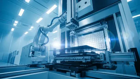
Manufacturing at the 2nm scale requires unprecedented precision in patterning silicon wafers. This is achieved through the next generation of Extreme Ultraviolet (EUV) lithography, specifically High-NA (Numerical Aperture) EUV systems. These advanced tools use a shorter wavelength of light and more sophisticated optics to etch the incredibly fine circuit patterns required for 2nm chips. The successful implementation of High-NA EUV is critical for achieving viable production yields and unlocking the full potential of the new node.
The Current State of 2nm Development and Production
Major foundries like TSMC, Samsung, and Intel are in a fierce race to master 2nm manufacturing. TSMC’s N2 process is reportedly on track for mass production, with major clients like Apple, Qualcomm, and MediaTek lining up to utilize the technology for their future flagship chips. However, the transition is not without difficulties, as initial reports indicate that manufacturers are grappling with low production yields due to the immense complexity of implementing GAA technology at scale.
Real-World Impact on Next-Generation Electronics
The primary application for early 2nm chips will be in flagship smartphones and high-performance computing. This technology will power next-generation processors such as Apple’s A20 for the iPhone 18 series, Qualcomm’s Snapdragon 8 Elite Gen 6, and MediaTek’s Dimensity 9600. For consumers, this translates to devices with faster processing speeds, more advanced AI capabilities, and longer battery life. Beyond mobile, 2nm will be crucial for developing more powerful and efficient CPUs and GPUs for data centers and AI accelerators.
The Economic and Manufacturing Hurdles
The Soaring Cost of Manufacturing
A significant challenge facing the 2nm node is the dramatic increase in manufacturing costs. The intricate processes involved with GAA transistors and advanced EUV lithography have led to a substantial rise in wafer prices. For example, the cost to produce Apple’s A20 chip is rumored to be nearly 80% higher than its predecessor. This price hike reflects the massive R&D investment and capital expenditure required to build and operate 2nm-capable fabrication plants.
Production Yield and Complexity Issues
The technical complexity of the 2nm process presents a major manufacturing hurdle. Achieving consistently high production yields with the new GAA architecture is proving to be difficult in the initial stages. Low yields directly translate to higher per-unit costs, as a larger number of chips on each wafer must be discarded. Overcoming these initial manufacturing pains is the key challenge for foundries to make 2nm production economically viable at a mass scale.
The Future Beyond the 2nm Node
The semiconductor industry is already looking past 2nm toward future nodes like 1.4nm (A14) and beyond. The successful implementation of GAA at 2nm serves as a foundational stepping stone for these future advancements. Future breakthroughs may involve novel materials like 2D semiconductors or new transistor structures like Complementary-FETs (CFETs) to continue the trend of miniaturization. The long-term impact will depend on balancing the relentless push for performance with the escalating economic and physical challenges of chip manufacturing.
Conclusion A Costly but Necessary Leap Forward
The 2nm process node represented a monumental achievement in semiconductor engineering, unlocking new levels of performance and efficiency through innovations like the Gate-All-Around transistor. It was a technology poised to power the next generation of cutting-edge devices. However, this progress came at a significant cost, with manufacturing complexities and soaring prices posing substantial challenges to the industry and, ultimately, to consumers. The 2nm era became a critical inflection point, one that redefined the economics of high-end electronics while paving the way for the computational advancements of tomorrow.