
The rapid acceleration of silicon fabrication and optical engineering has finally converged to push the modern smartphone beyond its long-standing architectural plateau. As the industry moves through the current development cycle, the roadmap for the iPhone 18 series reveals a departure from the safe, iterative updates of the past toward a model of aggressive vertical integration. This transition is not merely about faster speeds; it represents a fundamental reimagining of how a mobile device interacts with the physical world through advanced mechanical systems and proprietary telecommunications hardware.
Overview: The Strategic Shift in Development
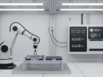
The current roadmap serves as a blueprint for the most ambitious hardware transition seen in recent years, moving firmly into the Production Validation Testing (PVT) phase. This stage is critical because it moves beyond theoretical design into the reality of mass manufacturing, where complex internal architectures must be proven viable at a global scale. By initiating these tests well ahead of the traditional autumn launch window, the objective is to iron out the logistical hurdles associated with entirely new material sciences and miniaturized mechanical components.
This shift signifies a move toward deep vertical integration that has been years in the making. Rather than acting as an integrator of third-party solutions, the development cycle focuses on bringing nearly every critical subsystem—from the modem to the camera’s physical iris—under a single engineering philosophy. This approach allows for a level of hardware-software synergy that competitors struggle to match, as every transistor and mechanical spring is optimized for a specific set of proprietary algorithms.
Pioneering Hardware: Processing and Optics
The A20 Pro Chipset: A 2nm Milestone
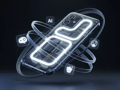
The A20 Pro application processor stands as the cornerstone of the Pro series, representing the first commercial implementation of a 2nm process node. By shrinking the transistor size even further, the goal is to deliver a leap in computational density that translates to more than just raw speed. This advancement functions to drastically reduce heat generation, which has historically been the primary throttle for sustained mobile performance. The increased efficiency allows for more complex on-device artificial intelligence tasks to run without the aggressive battery drain seen in previous 3nm generations.
Mechanical Variable Aperture: Physical Optics
Moving beyond the limitations of software-based image processing, the introduction of a mechanical variable aperture system mimics the functionality of the human eye. This component allows the lens to physically adjust its opening based on environmental lighting, providing a hardware-level solution to depth-of-field. The technical significance of this feature lies in its ability to produce natural bokeh through physical physics rather than digital interpolation. This results in superior focus across multiple planes in group photography and enhanced macro detail that retains a realistic texture often lost to AI sharpening.
Emerging Trends: Connectivity and Manufacturing
The latest developments highlight a strategic shift toward component independence and staggered product lifecycles. A major innovation is the introduction of the C2 chip, a second-generation in-house 5G modem. This reflects an industry-wide move toward reducing reliance on external suppliers, ensuring that the modem’s power consumption and signal acquisition are perfectly tuned to the device’s logic board. By controlling the modem stack, the architecture can switch between sub-6GHz and mmWave signals with much lower latency and thermal impact than generic, off-the-shelf solutions.
Furthermore, a new market strategy is emerging by decoupling the release dates of different models. The decision to stagger the launch of the base models away from the Pro series signals a change in how global supply chains and consumer demand are managed. This allows for a more focused allocation of the high-demand 2nm wafers to the premium devices initially, ensuring that the most advanced technology reaches the professional market without being diluted by the massive volume requirements of a simultaneous all-model launch.
Industrial Deployment: Real-World Applications
The technology within this roadmap is being deployed across several high-performance sectors, most notably in professional mobile filmmaking and high-speed telecommunications. In the creative industry, the variable aperture system offers tools that were previously reserved for dedicated DSLR equipment. This allows cinematographers to maintain consistent shutter angles while adjusting exposure physically, a workflow that was impossible on fixed-lens smartphones.
Additionally, the integration of the C2 modem ensures high-speed data deployment for enterprise users who require consistent connectivity in specialized private networks. In dense urban environments, the ability of the in-house modem to manage handoffs between different frequency bands more efficiently means fewer dropped packets during critical data transfers. This level of reliability is positioning the device not just as a consumer gadget, but as a legitimate tool for remote industrial monitoring and high-bandwidth field work.
Technical Hurdles: Scalability and Market Obstacles
Despite the projected advancements, the technology faces significant challenges regarding the manufacturing yields of 2nm wafers. Technical hurdles in mass-producing such delicate silicon at scale could lead to initial supply constraints or increased production costs that are passed on to the consumer. Furthermore, the high price point of emerging form factors, such as the rumored foldable variant designed to eliminate the screen “crease,” presents a market obstacle that may limit widespread adoption to a niche enthusiast group.
Rigorous PVT phases are currently being conducted to mitigate these limitations and ensure quality control. The complexity of a mechanical camera system also introduces new points of failure that fixed lenses do not have. Engineering a physical iris that can survive years of pocket lint, drops, and moisture requires a level of mechanical durability that is difficult to achieve in such a slim chassis. These trade-offs between mechanical sophistication and long-term ruggedness remain a central point of scrutiny for the engineering teams.
Future Trajectory: Long-Term Impact
The roadmap points toward a future where smartphones serve as highly specialized, professional-grade tools rather than general-purpose appliances. Potential breakthroughs in “creaseless” foldable displays and the continued refinement of in-house silicon suggest a move toward a completely integrated ecosystem where hardware and software are inseparable. Long-term, these advancements are likely to influence the broader electronics industry, setting new standards for what is expected from mobile processing power and mechanical durability.
As the industry moved through these developmental milestones, it became clear that the focus had shifted from “features” to “capabilities.” The transition to the A20 Pro and the C2 modem proved that vertical integration was the only path to overcoming the thermal and power efficiency ceilings of the previous decade. While the manufacturing complexities were immense, the successful implementation of these technologies established a new baseline for premium mobile hardware, forcing the rest of the market to reconsider their reliance on third-party silicon and fixed-lens optics. This cycle ultimately demonstrated that true innovation requires the courage to move back toward mechanical precision in a world that had become overly reliant on software patches.