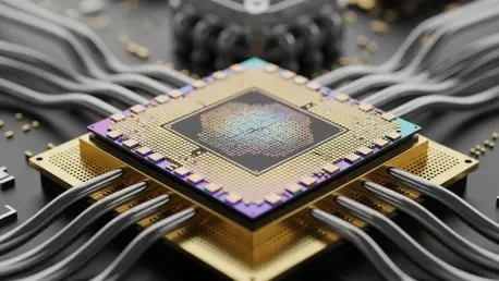

The shift from classical computing to quantum processing has exposed the reality that silicon, despite its dominance in the digital age, contains atomic-level imperfections that sabotage qubit longevity. In traditional complementary metal-oxide-semiconductor (CMOS) logic, a transistor remains functional even if a few atoms are displaced within the crystal lattice or if chemical impurities reside near the channel. However, quantum bits, or qubits, rely on the delicate superposition and entanglement of states that are extraordinarily sensitive to their immediate physical surroundings. Even the slightest fluctuations in electromagnetic fields, caused by nearby atomic defects, can trigger decoherence, effectively erasing the quantum information stored within the system. This transition from macro-scale reliability to micro-scale fragility has forced a total re-evaluation of how silicon wafers are sourced and processed. Engineering a reliable quantum processor now requires a level of material control that extends beyond the reach of standard commercial fabrication facilities currently operating in the global market.
The Influence of Isotopic Magnetic Noise
Natural silicon is primarily composed of the isotope Silicon-28, which is non-magnetic, but it also contains approximately 4.7 percent of the isotope Silicon-29. This specific isotope possesses a nuclear spin that creates a persistent and fluctuating magnetic environment often referred to as a magnetic bath. For spin qubits, which store information in the magnetic orientation of electrons, this bath acts as a constant source of background noise that causes the qubits to lose their phase coherence within microseconds. Researchers found that this isotopic noise is one of the most significant barriers to achieving the high-fidelity gates required for error correction in large-scale quantum arrays. To overcome this, the industry has begun utilizing isotopically purified silicon, which reduces the concentration of Silicon-29 to less than 0.001 percent. This purification process dramatically extends the coherence time of the qubits, allowing for more complex operations and providing a cleaner environment for quantum interactions.
Beyond the bulk properties of the silicon itself, the interfaces between the semiconductor and the insulating oxide layers represent another critical zone where atomic defects congregate. In a standard silicon-on-insulator architecture, the boundary where silicon meets silicon dioxide often harbors dangling bonds, which are atoms with unfulfilled chemical connections. These dangling bonds can trap and release individual electrons, creating charge noise that disrupts the electrical stability of the quantum dots used to define qubits. Furthermore, these traps can lead to two-level systems (TLS), which are microscopic defects that absorb energy from the qubits at specific frequencies. These interactions essentially steal the quantum state from the processor, leading to unpredictable errors during computation. Addressing these interface defects has necessitated the development of new passivation techniques that use hydrogen or deuterium to saturate the dangling bonds, thereby neutralizing their electrical activity and improving the overall stability of the quantum device.
Refining Manufacturing Standards for Sustained Quantum Reliability
The industry recognized that traditional fabrication methods were insufficient, leading to a pivot toward atomic layer deposition and specialized epitaxial growth to minimize structural irregularities. Engineers discovered that by carefully controlling the temperature and chemical precursors during the growth of silicon layers, they could significantly reduce the density of vacancies and interstitials that contribute to noise. This transition moved the focus from simple miniaturization toward the perfection of the crystal lattice itself, ensuring that each qubit resided in a nearly ideal environment. This shift allowed for the realization of higher-fidelity two-qubit gates, which were previously limited by the stochastic nature of material defects across the chip. These advancements demonstrated that the future of quantum scalability was not solely dependent on design architecture but was fundamentally tied to the chemistry of the substrate. By implementing these rigorous manufacturing standards, the sector established a baseline for consistency.
The adoption of localized noise spectroscopy became a standard practice for identifying problematic regions on a wafer before the final processor assembly was completed. This diagnostic approach allowed manufacturers to map out the distribution of defects and selected only the most pristine segments of the silicon for high-performance quantum modules. It was determined that a proactive strategy, involving the integration of material science at every stage of the design cycle, was the only viable path toward practical quantum advantage. By prioritizing the elimination of atomic-level noise through both material purification and sophisticated surface treatments, organizations successfully bridged the gap between experimental prototypes and reliable production units. The focus ultimately settled on creating a holistic ecosystem where the software layer accounted for residual hardware imperfections while the hardware itself pushed the limits of atomic precision. This integrated methodology ensured that the industry remained on track to deliver robust systems.