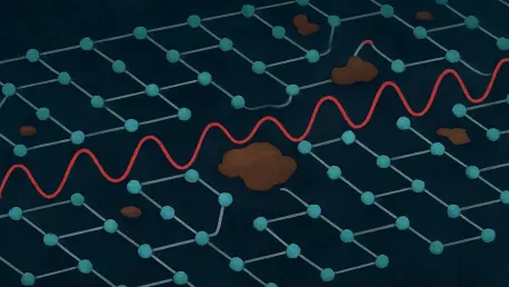

The conventional understanding of electricity suggests that impurities and structural flaws within a material should hinder the flow of electrons, acting as obstacles that increase resistance and degrade performance. While this classical view holds true to a point, the bizarre rules of quantum mechanics allow for a far more dramatic outcome. With enough precisely placed disorder, electrons do not just slow down; they can become completely trapped, their wave functions interfering destructively to create invisible prisons that halt their movement. This phenomenon, known as Anderson localization, transforms a conductor into an insulator not through a change in its fundamental composition, but through the strategic introduction of chaos. For decades, directly observing and controlling this transition in a two-dimensional material has been a significant challenge for physicists, requiring a level of atomic-scale precision that was difficult to achieve. Graphene, with its unique electronic properties and single-atom thickness, has long been a theoretical candidate for exploring this quantum effect, but identifying the exact threshold where disorder ceases to be a mere nuisance and becomes a tool for manipulating electron behavior has remained an elusive goal.
1. Systematically Creating Defects
A recent study published in ACS Nano provides the most direct experimental evidence to date of this quantum phenomenon in single-layer graphene, demonstrating not only the onset of Anderson localization but also its ability to enhance the material’s thermoelectric properties. The research, conducted by a team primarily from Clemson University and the College of Charleston, centered on a methodical approach to introducing and quantifying disorder. To achieve this, the scientists employed argon-ion irradiation, a technique that bombards the graphene surface with ions to create vacancy defects with high precision. By carefully controlling the irradiation power and exposure time, they were able to produce a series of samples that spanned a wide spectrum of disorder levels. The key to the experiment was not just creating these defects but also measuring them accurately. The team used Raman spectroscopy, a powerful analytical technique that measures how light scatters off a material’s atomic vibrations. The ratio of two specific peaks in the Raman spectrum—the disorder-induced D-band and the intrinsic G-band—served as a reliable fingerprint for the average spacing between defects, a parameter known as the interdefect distance, L_D. This allowed the researchers to map their experimental results to a precise, quantifiable structural property, with L_D values across their samples ranging from approximately 10 to 60 nanometers.
2. A Critical Threshold for Quantum Effects
The central breakthrough of the research was the discovery of a sharp, critical threshold at an interdefect distance of approximately 20 nanometers (L_D* ≈ 20 nm). At this precise point, multiple independent measurements revealed a fundamental shift in the way electrons travel through the material. To probe this transition, the team used ultrafast pump-probe reflectivity, a technique that involves hitting the graphene with an extremely short laser pulse (50 femtoseconds) and then tracking how quickly the excited electrons relax back to their equilibrium state. The measurements showed that the relaxation times peaked dramatically right around the 20 nm defect spacing. In pristine or lightly disordered graphene, electrons behave as highly mobile, delocalized particles. However, as the defect density increases to the critical threshold, quantum interference effects begin to dominate, trapping electrons in localized spatial pockets. Instead of flowing freely, transport now relies on a much slower process of thermally activated “hopping” from one localized state to another. This hopping mechanism became the dominant relaxation pathway at the 20 nm threshold, causing the observed peak in relaxation times. Further temperature-dependent measurements supported this conclusion, showing that the peak persisted down to 173 K but vanished at 123 K as the thermal energy required for hopping was “frozen out,” confirming the quantum nature of the observed transport behavior.
3. Corroborating Evidence and Theoretical Validation
To solidify their experimental findings, the researchers turned to theoretical modeling and additional electrical measurements. Using the kwant quantum transport package, they ran tight-binding simulations that modeled the graphene lattice at an atomic level. By systematically removing carbon atoms to simulate defects, they could compute the spatial distribution of the electron wave functions. In the model of pristine graphene, the charge was spread evenly across the entire structure, representing delocalized electrons. However, once the defect density crossed a threshold corresponding to the experimentally observed 20 nm spacing, the simulation showed the wave function collapsing into isolated, high-probability lobes surrounded by areas of near-zero charge density. This provided a clear visual and theoretical confirmation of spatial localization. This evidence was further corroborated by electrical resistivity measurements performed on a separate set of graphene samples. As the interdefect distance L_D dropped below 20 nm, the material’s resistivity increased exponentially. Concurrently, the temperature dependence of the resistivity shifted from metallic behavior (where resistivity is nearly constant) to insulating behavior (where resistivity decreases as temperature rises), a classic signature of transport dominated by thermally activated hopping between localized states. This convergence of optical measurements, electrical data, and theoretical simulations provided a robust and multi-faceted confirmation of the Anderson localization threshold in graphene.
4. A New Blueprint for Material Design
The implications of this controlled localization extended beyond fundamental physics into the realm of energy conversion. The study revealed that the material’s thermoelectric performance was not degraded but significantly enhanced right at the critical disorder threshold. The Seebeck coefficient, which measures the voltage generated from a temperature difference, rose steadily as the defect density increased. More importantly, both the thermoelectric power factor and the figure of merit, zT, which are key metrics of a material’s efficiency in converting heat to electricity, reached a pronounced maximum precisely at the L_D* ≈ 20 nm spacing. This counterintuitive result—where adding defects improves performance—aligns with a theoretical prediction made by Mahan and Sofo in 1996. They argued that optimal thermoelectric materials should function as sharp energy filters, allowing charge carriers at specific, favorable energies to pass through while blocking others. Anderson localization achieves exactly this. Near the threshold, the electronic states form narrow energy bands that selectively transmit electrons, boosting the Seebeck coefficient without a proportional increase in electrical resistivity. Although graphene’s inherently high thermal conductivity prevents it from becoming a practical thermoelectric material, its value in this study was as a perfectly transparent model system. The research provided the clearest experimental link yet between a quantifiable disorder level and localization-enhanced thermopower in a 2D material, a connection that has remained indirect in more complex bulk materials. The findings established a powerful design principle: disorder, when precisely engineered, can be harnessed as a tool to tune quantum transport and optimize energy conversion, paving the way for novel approaches in designing next-generation thermoelectric and electronic devices.