
The rapid evolution of optical technologies has long been hindered by the staggering computational costs associated with simulating how light interacts with structures smaller than its own wavelength. Engineers attempting to design the next generation of ultra-thin optical devices have historically faced a brutal reality: solving Maxwell’s equations for complex geometries requires immense computational power and days, or even weeks, of processing time for a single iteration. This bottleneck has significantly stifled innovation across various sectors, as the trial-and-error cycle of nanophotonic design remained prohibitively expensive for smaller research firms. However, a significant shift is occurring as researchers at Chalmers University of Technology move away from standard, data-hungry machine learning models toward a more sophisticated physics-informed approach. By embedding fundamental laws directly into the neural network architecture, scientists are now able to bypass the traditional data-generation hurdle effectively.
Integrating Physical Laws into Machine Learning
Mathematical Foundations: Implementing Quasinormal Mode Expansion
To address the persistent delays in optical simulation, the research team integrated a specialized theoretical framework known as quasinormal mode expansion directly into the core of the neural network’s design. This approach allows the system to understand the natural resonances of light within a structure as a fundamental property rather than a random pattern to be discovered through brute-force data analysis. By framing electromagnetic behavior through these specific resonances, the researchers ensured that the AI model is naturally constrained by the established rules of physics. This mathematical grounding provides a rigid structure that prevents the neural network from straying into unphysical territory during its calculation phases. Consequently, the model does not just predict outcomes based on statistical probability but arrives at solutions that are fundamentally rooted in the way light actually behaves in a physical environment, ensuring high reliability.
Integrating these physical constraints means the artificial intelligence inherently respects principles like energy conservation and causality by default without needing additional supervision. In standard machine learning models, which are often described as black boxes, the system might generate predictions that look plausible but are physically impossible, such as a lens that produces more energy than it receives. By hard-coding the constraints of Maxwell’s equations into the training architecture, the Chalmers scientists have eliminated the risk of these unrealistic outputs. This shift from purely statistical learning to physics-informed learning transforms the AI from a mere pattern-recognition tool into a digital physicist. This structural integrity is particularly vital for researchers who require high-precision results for sensitive applications, where even a minor calculation error could lead to the failure of an entire hardware system.
Resource Management: Streamlining the Training Pipeline
This innovative structural shift has led to extraordinary efficiency gains in how these models are prepared for real-world application, specifically by reducing data needs. Historically, the most significant barrier to using AI in photonics was the sheer volume of training data required, often involving tens of thousands of high-fidelity simulations. The physics-informed model, however, has demonstrated the ability to achieve superior accuracy while requiring up to 90 percent less training data than its conventional counterparts. For specific structures, such as photonic crystal slabs, the network reached a state of high operational precision with only 160 training examples. This drastic reduction in data dependency allows research teams to move forward without the massive server farms typically associated with large-scale machine learning projects, democratizing access to high-end design capabilities for smaller institutions.
Beyond just reducing the volume of data, this methodology has fundamentally altered the project timelines for developing new nanophotonic components. Previously, the data generation phase alone could consume an entire month of non-stop supercomputing time, creating a massive lag between the initial concept and the testing phase. With the new physics-informed framework, this timeframe has been compressed from thirty days to just three days, representing a tenfold increase in development velocity. This acceleration is crucial in a fast-paced market where the window for innovation is narrow and the demand for new consumer technology is constant. By shortening the feedback loop, engineers can now afford to take more creative risks, exploring radical new geometries that were once considered too computationally expensive to even simulate, let alone optimize, through traditional iterative design methods.
Achieving Operational Speed and Design Flexibility
Performance Optimization: The Shift to Inverse Design
Once a physics-informed neural network has been fully trained and validated, its ability to analyze optical properties happens almost instantaneously. This near-instantaneous inference speed enables a powerful design methodology known as inverse design, which represents a total reversal of the traditional engineering workflow. In a traditional setup, a designer would propose a shape and then check its performance; with inverse design, the researcher provides the desired optical performance, and the AI suggests the exact physical structure needed to achieve it. Because the network can process these queries in less than a second, it allows for a real-time exploration of the design space that was previously impossible. Engineers can now cycle through hundreds of different performance targets in a single afternoon, pinpointing the optimal configuration for a specific task with unprecedented accuracy and speed.
This synergy between technological speed and human expertise is essential for navigating the extreme complexities of light interaction at the nanoscale. While human physicists have a profound understanding of the underlying equations, the way light twists and scatters through intricate, multi-layered shapes is often too complex for human intuition alone to manage effectively. The AI serves as a sophisticated computational bridge, taking the fundamental physical rules provided by the expert and applying them to complex design challenges that would otherwise remain opaque. This relationship allows the researcher to focus on high-level conceptual goals while the machine handles the grueling mathematical translations required to realize those goals. It creates a collaborative environment where the machine’s processing power and the human’s creative vision work in tandem to push the boundaries of what is possible in optical engineering.
Industrial Application: Realizing the Potential of Nanophotonics
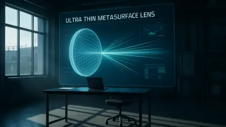
The practical applications of these accelerated design processes are far-reaching and are already beginning to impact fields like imaging and quantum communications. By utilizing these AI-designed metasurfaces, manufacturers are now capable of creating camera lenses that are significantly thinner and lighter than those found in current mobile devices. These flat lenses, often only a few hundred nanometers thick, can perform the same functions as bulky glass elements while reducing the overall footprint of the device hardware. Furthermore, these designs are becoming indispensable for the development of quantum computing systems, where precise control over light signals is necessary for transporting data reliably. As the industry moves toward 2027 and 2028, the ability to integrate high-efficiency optical components into compact chips will be a primary driver for next-generation computing platforms.
The implementation of physics-informed artificial intelligence marked a definitive turning point in the field of nanophotonic design by resolving the longstanding conflict between accuracy and speed. By moving away from massive, unstructured datasets and embracing the rigid constraints of electromagnetic theory, researchers established a more sustainable and accessible development model. This transition allowed for the rapid prototyping of metasurfaces and quantum components that once required months of preparation. Organizations that adopted these hybrid computational strategies found themselves better positioned to meet the escalating demands for miniaturized high-performance hardware. Moving forward, the focus shifted toward refining these models for even more complex, non-linear materials and integrating them directly into automated fabrication lines. This progress demonstrated that the true power of AI in science lies not in replacing fundamental laws, but in mastering them.