
The dramatic revitalization of Intel Corporation throughout the opening months of this year has fundamentally altered the competitive landscape of the semiconductor industry, driven by a seventy percent surge in stock value and a series of high-profile industrial alliances. This resurgence marks a significant departure from the company’s historical reliance on consumer-grade processors, signaling a decisive shift toward specialized manufacturing ecosystems and sophisticated cloud infrastructure. By positioning itself at the intersection of high-scale artificial intelligence and aerospace computing, the firm has moved beyond its traditional identity as a chipmaker to become a vital architect of the most demanding technical environments. Central to this transformation is a strategic pivot that emphasizes balanced system architectures over raw hardware acceleration, a move designed to address the complex bottlenecks currently facing global data centers. This trajectory reflects a broader corporate evolution, focusing on the specialized requirements of a new era defined by massive computational demands and the physical rigors of orbital environments.
Strategic Foundations: The Evolution of Cloud Infrastructure
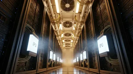
The ongoing collaboration with Google Cloud serves as a primary pillar for this new strategic direction, focusing on the continued refinement of Xeon processors and advanced Infrastructure Processing Units. This partnership represents a shift toward a more holistic view of data center performance, where the priority is no longer just the central processing unit but the efficiency of the entire ecosystem. By offloading critical networking, storage, and security tasks to specialized Infrastructure Processing Units, the system allows the main processors to focus entirely on the primary computational workloads. This methodology, often referred to as building balanced systems, directly addresses the inefficiency of modern AI environments where data movement frequently outpaces processing speed. Such architectural improvements are essential for managing the sheer volume of information required for large-scale machine learning, ensuring that the hardware does not become a hindrance to the growth of cloud-based services.
Moreover, this focus on offloading and optimization addresses the critical sustainability challenges that have historically plagued massive data center operations. As energy costs and environmental regulations become more stringent, the ability to reduce power consumption while maintaining high throughput has become a competitive necessity. The current strategy aims to provide a path toward carbon-neutral computing by streamlining how data flows through the silicon, minimizing wasted heat and energy. This technological advancement allows providers like Google to offer more robust services without an exponential increase in physical footprint or power draw. By integrating these efficiencies into the core of the cloud fabric, the industry moves closer to a sustainable model for artificial intelligence that does not sacrifice performance for environmental compliance. This systemic approach ensures that the infrastructure remains resilient and adaptable to the evolving needs of global enterprises seeking reliable and scalable AI solutions.
Material Innovation: Gallium Nitride and the Terafab Era
The most transformative development in this technological pivot involves the integration into the Terafab initiative, an ambitious project led by Elon Musk to achieve one terawatt of annual computing capacity. This project dwarfs existing global production capabilities and requires a radical rethinking of how semiconductors are designed and manufactured at scale. A cornerstone of this effort is the breakthrough in gallium nitride chiplet technology, which has allowed for the successful integration of high-voltage power electronics with silicon logic circuits on a single 300mm wafer. This engineering feat represents a massive leap forward in material science, as gallium nitride offers thermal and electrical properties that far exceed those of traditional silicon. By merging these two distinct functions on a single substrate, the design eliminates the need for separate components, significantly reducing the overall footprint and complexity of the hardware required for massive AI clusters.
The resulting chiplets are remarkably thin, measuring approximately nineteen microns, which is roughly one-fifth the thickness of a human hair. This extreme miniaturization does not come at the expense of durability; in fact, the use of gallium nitride provides superior resistance to intense heat and radiation. These physical properties are essential for the high-density environments of the Terafab project, where thousands of chips must operate in close proximity without failing due to thermal stress. Furthermore, the ability to produce these chips on standard 300mm wafers ensures that the manufacturing process can be scaled efficiently using existing foundry infrastructure. This marriage of high-voltage power management and logic processing in a compact, resilient package solves many of the hardware limitations that have previously capped the growth of large-scale artificial intelligence, paving the way for a new generation of supercomputing facilities capable of handling unprecedented workloads.
Final Frontiers: Spaceborne Processing and Market Realities
The strategic value of this gallium nitride technology extends far beyond terrestrial data centers, finding a critical application in the burgeoning aerospace industry and the specific needs of SpaceX. In the context of space exploration, where every pound of cargo carries a massive financial cost, the ability to combine power and logic into a lightweight, durable package provides an immense economic advantage. These specialized chips are expected to support space-based artificial intelligence processing and the creation of industrial infrastructure in orbit. The inherent resistance to radiation and extreme temperature fluctuations makes these processors ideal for long-term deployment in the harsh environment of space, where standard silicon often fails without heavy and expensive shielding. This capability allows for more sophisticated onboard decision-making for satellites and spacecraft, reducing the reliance on long-distance communication with ground stations and enabling real-time autonomy in deep-space missions.
Despite these significant technological milestones and the dramatic rally in stock price, professional valuation and market sentiment have remained somewhat divided. While the engineering breakthroughs are undeniable, many analysts maintained a cautious stance, often issuing hold ratings with price targets that lagged behind the current market performance. This discrepancy suggested that while the company successfully positioned itself as a leader in specialized computing, concerns remained regarding whether the earnings potential would ultimately justify the rapid appreciation in share value. Nevertheless, the strategic direction established throughout this period provided a clear roadmap for future development in both AI and aerospace. Stakeholders looked toward the continued integration of power and logic as a solution to terrestrial energy constraints and orbital hardware challenges. The move toward becoming a foundational architect of specialized systems was solidified as the primary pathway for maintaining long-term industry relevance and technological leadership.