In a paper co-authored by Harvard University researchers to pioneer next-generation AI semiconductor technology, Samsung Electronics has recently expressed a vision for a chip that emulates the human brain In the coming years, neuromorphic computing could prove extremely vital for solving specific technical challenges, such as effectively implementing Artificial Intelligence.
What Is Neuromorphic Computing?
As traditional semiconductors reached the limits of miniaturization and capacity, researchers turned their heads towards a new approach to semiconductor design: neuromorphic computing powered by neuromorphic chips.
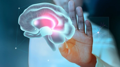
Neuromorphic computing is a complete rethinking of computer architecture from the bottom up. The technology mimics the physics of the human brain and nervous system by mapping spiking neural networks and copying them onto memory chips. The ultimate goal of this technology is to apply the latest insights from neuroscience to create chips that function less like traditional computers and more like the human brain.
Although getting computing devices to think creatively and recognize foreign people or objects is still a distant goal. In recent years, tech giants including Samsung, Intel, HP, and IBM, as well as government research hubs like Sandia National Laboratories and academics worldwide, started exploring this new technology.
Moreover, Emergen Research says the global neuromorphic processing market will reach $11.29 billion by 2027.
One Step Closer to Making Chips that Can Mimic the Human Brain
Conceived by engineers and researchers at Samsung and Harvard University, this insight was the subject of a scientific paper entitled “Neuromorphic electronics based on copying and pasting the brain,” which was published in Nature Electronics.
The essence of the vision could be best described by the two words: “copy” and “paste”. The paper describes a way to copy the brain’s neural connection map using a nanoelectrode array, discovered and developed by Dr. Ham and Dr. Park, and paste it onto a three-dimensional, high-density solid-state memory array. Through this copy-and-paste approach, the authors intend to create a memory chip that exucdes the unique computational traits of the brain that may not be within the reach of current technology, such as low power, easy learning, environmental adaptation, and even autonomy and cognition.
The brain is made up of a large number of neurons, and their wiring map is responsible for brain functions. Thus, authors state that the knowledge of the map is the key to reversing brain engineering.
Downloading the Brain’s Neural Connection Map onto a Memory Chip
Launched in the 1980s, the original goal of neuromorphic engineering was to mimic the structure and function of neural networks on a silicon chip. This has proved difficult to achieve, as even today little is known about how neurons are wired to create higher brain functions. Thus, the goal of neuromorphic engineering has been facilitated by designing a chip ‘inspired’ by the brain, rather than rigorously mimicking it.
The paper suggests a way back to the original neuromorphic goal of reverse engineering the brain. The nanoelectrode array can actually record electrical signals from high sensitivity neurons. These intracellular recordings design the map of neuronal wiring, indicating where neurons connect to each other and the strength of these connections. From these recordings, the neuronal wiring map can, therefore, be extracted or ‘copied’.
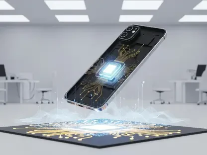
The copied neuronal map can then be pasted into a network of non-volatile memories – such as the commercial flash memories that we use every day as physical storage drives (SSDs) or new memories, such as resistive random access memories (RRAMs). This transfer can be done by programming each memory so that its conductance represents the strength of each neuronal connection in the copied map.
The scientific paper goes even further and suggests a method to paste the neural wiring map onto a physical memory network. This involves a non-volatile random-access memory network specifically designed to learn and express the neuronal connection map when directly driven by the recorded intracellular signals. This is the method Samsung thinks will allow us to directly download the brain’s neural connection map onto a memory chip.
An Extremely Ambitious Vision
The human brain has approximately 100 billion neurons and about a thousand times as many synaptic connections. Thus, the ultimate neuromorphic chip will have to accommodate 100 trillion virtual neurons and synapses. Integrating such a large number of memories on a single chip would only be possible through 3D memory integration, a technology designed by Samsung that has opened a new era in the memory storage industry.
“The vision we are presenting is extremely ambitious. But working toward such a heroic goal will push the boundaries of machine intelligence, neuroscience, and semiconductor technology,” said Dr. Ham, a partner at Samsung Advanced Institute of Technology (SAIT) and Harvard University professor.


