
The global transition toward sustainable energy sources has reached a critical juncture where traditional silicon-based photovoltaics are rapidly approaching their theoretical efficiency limits, necessitating the development of next-generation materials like perovskites. While these materials promise a revolution in how sunlight is captured, the path from successful laboratory prototypes to mass-produced modules has been hindered by the delicate nature of the chemical processes involved in their creation. A major collaborative effort between The Hong Kong University of Science and Technology and the University of Oxford has now demonstrated a way to bypass these obstacles through a sophisticated vacuum-based manufacturing technique. This research, recently detailed in the journal Nature Materials, provides a definitive blueprint for producing high-efficiency solar cells without the volatile solvents that have long plagued the industry. By refining the vacuum-deposition process, the team has managed to create a stable, reproducible, and highly efficient solar architecture that fits perfectly into existing industrial manufacturing pipelines, marking a significant shift in renewable energy strategy.
Transitioning from Liquid Inks to Industrial Vacuum Processes
For years, the most efficient perovskite solar cells were fabricated using solution-processed methods, which involve dissolving the precursor materials in liquid solvents to create an ink that is then coated onto a surface. Although this wet approach works exceptionally well for small-scale experiments, it becomes increasingly problematic when attempting to cover the large areas required for commercial solar panels. The evaporation of solvents often results in uneven film thickness and structural defects, which compromises the overall performance of the device. Furthermore, the use of toxic or volatile organic solvents introduces significant environmental and safety concerns for large-scale factories, requiring complex waste management systems. These challenges have traditionally created a scaling gap where the high performance seen in the lab is difficult to replicate on a production line. Consequently, finding a solvent-free alternative has become a top priority for researchers aiming to commercialize this technology for the power grid.
Vacuum deposition offers a compelling solution to these manufacturing hurdles by utilizing a dry process that is already standard in the production of high-end electronics like organic light-emitting diode (OLED) displays. This method involves heating materials in a vacuum chamber until they sublimate and condense onto a substrate, ensuring a uniform and highly controlled coating across large surfaces. Unlike liquid-based methods, vacuum deposition avoids the unpredictability of solvent drying and allows for the precise layering of different materials with nanometer-scale accuracy. Despite these clear industrial advantages, vacuum-deposited perovskites historically suffered from poor crystal quality and lower efficiencies compared to their liquid-processed counterparts. The lack of control over how the crystals formed in a vacuum often led to high defect densities, which acted as barriers to electrical current. Bridging the performance gap between these two methods required a fundamental reimagining of the vacuum-co-evaporation process at the molecular level.
Molecular Engineering: Controlling Crystal Growth and Alignment
The breakthrough achieved by the collaborative research group hinges on a sophisticated multi-source co-evaporation technique that introduces a lead chloride additive as a secondary source during the deposition. This additive plays a crucial role as a structural director, guiding the assembly of the perovskite lattice as the individual molecules settle onto the substrate. By carefully tuning the ratio of these precursors, the researchers were able to influence the kinetics of the crystal formation, ensuring that the material grows in a highly ordered fashion. This method effectively instructs the atoms to arrange themselves into a specific crystalline structure that is optimized for photovoltaic performance. The presence of the chlorine-based director prevents the chaotic, random crystallization that typically occurs in standard vacuum processes, leading to a much cleaner and more predictable material. This level of control is essential for creating high-performance devices that can be manufactured reliably at a massive scale without the need for constant recalibration.
A defining characteristic of this new material is the specific (100) face-up orientation of the perovskite grains, which provides a smoother pathway for charge carriers to move through the solar cell. This structural alignment significantly reduces the density of traps, which are microscopic imperfections where electrons often lose energy and get stuck before they can be harvested as electricity. Beyond improving energy conversion efficiency, this ordered orientation enhances the mechanical and chemical stability of the film. When the crystals are aligned in this manner, the material becomes much more resilient to the environmental stressors that typically cause perovskites to degrade, such as prolonged exposure to heat and intense sunlight. By addressing the root cause of both efficiency loss and instability, the research team has created a wide-bandgap perovskite that possesses the durability required for long-term outdoor use. This structural improvement represents a fundamental shift in how scientists approach the design of thin-film photovoltaics for industrial applications.
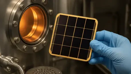
Performance Benchmarks and Rigorous Durability Testing
The efficacy of this new vacuum-deposition method is reflected in the record-breaking performance metrics documented during the study, particularly for wide-bandgap perovskite cells. The research team successfully developed a device that achieved a certified maximum-power-point-tracked efficiency of 18.35%, with some laboratory-tested versions reaching as high as 19.3%. These figures are particularly impressive because they were achieved in a wide-bandgap configuration, which is essential for tandem solar cell designs. Furthermore, the technology showed exceptional scalability, maintaining an efficiency of 18.5% even as the cell size was increased to one square centimeter. This stability in performance across different device sizes is a strong indicator that the process is robust enough for industrial transition. Many laboratory breakthroughs fail when they are scaled up, but the vacuum co-evaporation technique demonstrated here maintains its integrity. This success proves that the historical gap between solution-processed and vacuum-deposited cells is finally closing.
Durability remains the primary concern for the solar industry, and the vacuum-deposited cells underwent rigorous testing to prove their resilience under harsh environmental conditions. Following the International Summit on Organic Photovoltaic Stability protocols, the encapsulated devices were subjected to continuous full-spectrum sunlight and high temperatures in an ambient air environment. After more than 1,000 hours of continuous exposure, the cells managed to retain over 80% of their initial peak performance, showcasing a level of stability that rivals the best liquid-processed perovskites. This resilience is a direct result of the highly ordered crystal structure, which prevents the internal chemical migration that typically destroys perovskite cells. By demonstrating that these cells can survive extreme thermal and light-induced stress, the researchers have provided the necessary evidence that vacuum-deposited perovskites are ready for real-world deployment. This level of reliability is critical for attracting the investment needed to build the first generation of commercial perovskite factories.
Advanced Diagnostics and Real-World Implementation
To understand why this new manufacturing method was so effective, the research team utilized operando hyperspectral imaging, a sophisticated diagnostic tool that maps the optical signals of a working solar cell. This spectral camera allowed the scientists to observe the internal physics of the device in real-time, identifying exactly where energy was being converted efficiently and where it was being lost to defects. By visualizing the behavior of the cell on a pixel-by-pixel basis, they were able to distinguish between beneficial charge recombination and detrimental pathways like halide segregation. This diagnostic insight confirmed that the lead chloride additive successfully eliminated the chemical instabilities that often plague multi-element perovskites. The ability to see these microscopic processes while the cell is actually generating power provides a powerful roadmap for further optimization. This scientific approach ensures that future improvements to the technology will be based on hard data rather than trial-and-error experimentation.
The most exciting application of this high-quality perovskite film is in the creation of tandem solar cells, which combine perovskite and silicon layers to maximize energy harvest. Because vacuum deposition creates a conformal coating, it can perfectly cover the microscopic, pyramid-like textures found on standard industrial silicon wafers. This allows the perovskite layer to capture high-energy blue light while the underlying silicon captures the lower-energy red and infrared light. The team produced 1 cm² tandem cells with a remarkable efficiency of 27.2%, which were then tested in an eight-month outdoor trial in Italy. During this extensive field test, the cells maintained approximately 80% of their original performance, proving they can withstand the fluctuations of a real-world environment. These results established that the transition from a controlled laboratory setting to an unpredictable outdoor climate was entirely feasible. This milestone suggested that the technology was mature enough for manufacturers to begin integrating vacuum-deposited perovskites into existing solar module production lines.